Empowering Generative AI at the Edge: Unveiling the SAKURA-II Benefits

{% module_block module "widget_1d6e0a79-7de3-4243-b2f9-60fa1bff70c2" %}{% module_attribute...
As a continuation to a previous report on the Linley Fall Processor Conference 2020. This time, however, there will be a big difference — we at EdgeCortix participated in this edition of the Linley conference and officially unveiled our hardware and software technology for low-latency and low-power AI inference at the edge.
I will first cover our talk, and then summarize other AI-related talks from the conference. Similar to the report on the previous edition, talks that were not specifically targeted at AI acceleration might be missing from this article.
EdgeCortix’s technology stack presentation was composed of two major parts. The first is the Dynamic Neural Accelerator™ (DNA) IP which is a modular, scalable, low-latency and low-power IP for AI inference at the edge using Deep Neural Networks (DNN). The second part is the Multi-module Efficient Reconfigurable Accelerator (MERA) compiler and SDK that provides a seamless user experience for machine learning engineers, allowing them to target our DNA IP in the same way as they would target a CPU or GPU. MERA natively supports standard machine learning frameworks such as PyTorch, TensorFlow & TensorFlow Lite, while transparently ensuring that the compute capability of the DNA IP is utilized to the maximum extent possible regardless of the size or configuration of the IP. MERA supports INT8 quantized models directly in the machine learning framework, with no custom quantization or re-training of the models being required.
EdgeCortix’s technology stack is specifically optimized to tackle the problem of low compute utilization that plagues many existing AI accelerators, especially when it comes to small-batch and batch-1 inference which are crucial for inference at the edge. The solution to this challenging problem is two-fold:
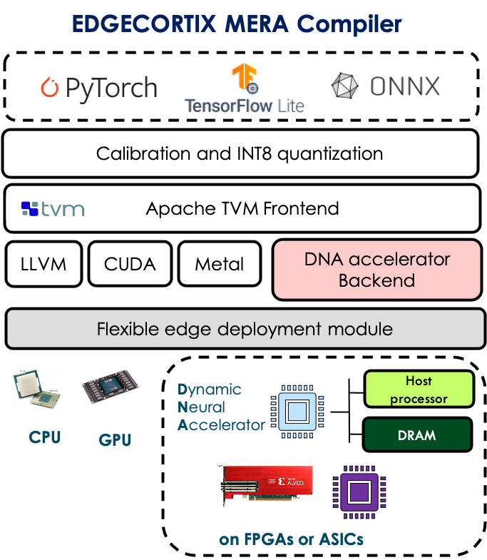 EdgeCortix MERA Compiler & Software Stack (image from official Presentation)
EdgeCortix officially unveiled the DNA-A series IP product line at the Linley conference, which is composed of 5 pre-determined single core configurations of our IP covering the peak compute performance range of 1.8 to 54 INT8 TOP/s, while using less than 0.6 Watts in the smallest case and less than 8 Watts in the largest case, assuming an operating frequency of 800 MHz using TSMC 12 nm fabrication technology. Needless to say, the IP is fully configurable, allowing users the ability to adjust the number and size of the different compute components in the IP, and also the amount of on-chip memory available, based on their own specific needs.
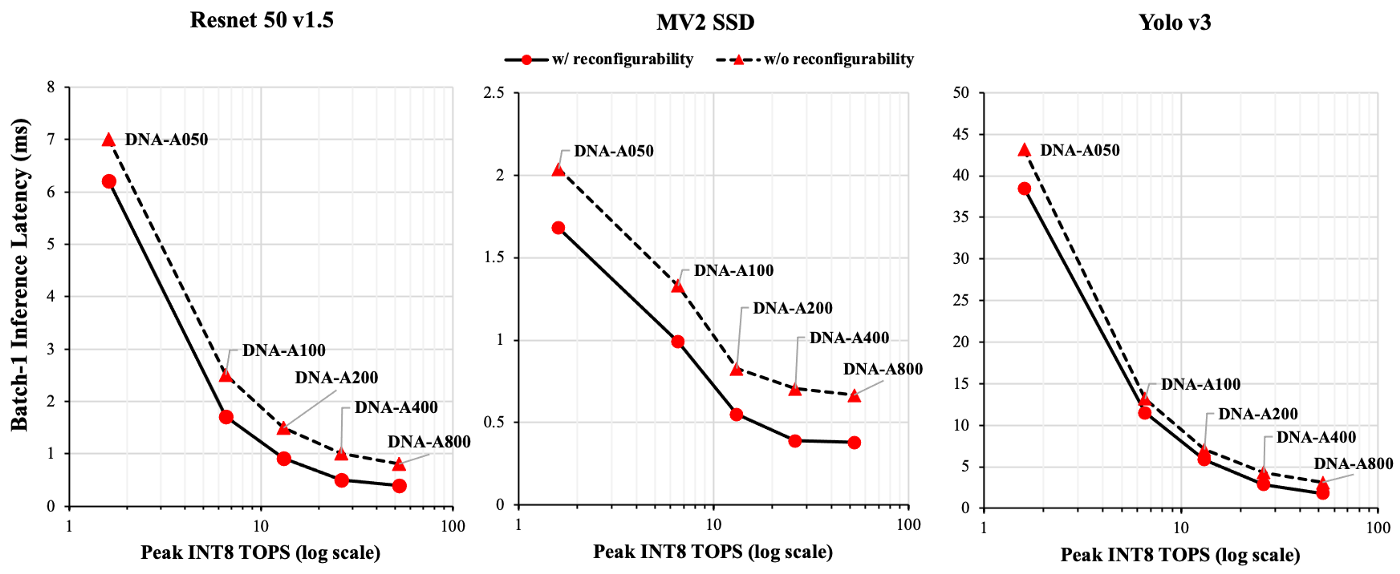
EdgeCortix is currently in the process of taping out the first AI chip as part of a PCI-E board with LPDDR4 memory modules, using the 54-TOP/s DNA-A800 configuration, which is expected to achieve a batch-1 inference throughput of 2500, 2600, and 555 IPS (Images per second) for Resnet 50 v1.5 (224x224), Mobilenet v2 SSD (MV2 SSD 300x300), and Yolo v3 (416x416) neural networks, respectively, while consuming less than 10 Watts in total board power. More details about EdgeCortix’s IP and performance appeared in the recent Linley Group Microprocessor Report.
Now let’s look at the rest of the presentations in the conference.
Similar to the previous conference, DeepAI again talked about their 8-bit-quantized training process accelerated on FPGAs. However, they did not really say much new and their presentation this time was even more high-level than the previous one. They did report some accuracy numbers this time from their fixed-point 8-bit training and standard FP32 training on GPUs, pointing to less than 0.3% loss of accuracy when doing 8-bit classification training using Resnet 50, and no loss of mAP when doing 8-bit object detection; re-training using Tiny Yolo v3 compared to FP32. Though they seem to be mostly targeting the retail sector and focusing on related datasets such as fruits and grocery items; it is not clear how their 8-bit training would perform on more critical vision applications such as in self-driving cars or mobile robots.
Expedera came out of stealth mode and introduced their neural network engine for inference at the edge. They claimed the use of principles of packet switching ASICs from the networking domain in their design, and moved all the software complexity such as neural network decomposition, dependency analysis, scheduling and resource management to the hardware, to the point that instead of a compiler, they use a “translator” to convert a given neural network to the format that would run on their hardware.
Their presentation was quite high-level and low-level details were scarce; the only useful but vague thing they said about the hardware was that it uses a deep pipeline design with no synchronization or backpressure, and deterministic latency. They provide a monolithic IP that scales from 1 TOP/s to 100 TOP/s and supports INT8 and INT16/FP16. Currently, it seems they only support Tesnorflow/TFLite. They claimed an IPS/W of 2010 for Resnet 50 inference with their taped-out chip at TSMC 7 nm. However, there was no mention of the batch size in the presentation. Reading the Linley report on them that came out at the same time as the conference, shows that the IPS/W they are claiming is not actually for the IPS/W of their full 32 TOP/s chip, but is the IPS/W after turning off some compute tiles in the chip to reduce the peak performance to 8 TOP/s. Moreover, the number is actually at a batch size of 16 instead of 1, which doesn’t make much sense for edge workloads and does not align with all their claims on having higher utilization compared to their competitors; it is possible to get high utilization with a batch size of 16 even on massive GPUs.
Hailo presented the latest status of their hardware and software and it seems they have finally managed to deliver some reasonable numbers. They reported a peak performance of 26 INT8 TOP/s for their chip, achieving 1223 FPS on Resnet 50 at 3 Watts; albeit they did not mention the batch size. Strangely enough, they quoted MLPerf results to complain about other people’s unrealistic boasting, while MLPerf is exactly supposed to prevent this by providing a fair benchmarking environment where everyone’s hardware can be benchmarked under the same conditions to get comparable results, and their chip happened to perform very poorly in MLPerf (they only submitted to v0.5, though). They also mentioned some performance numbers such as Yolo v5 (640x640) running at 191 FPS with 6 independent streams (batch size = 6) with under 4 Watts of power usage, Mobilenet v1 (300x300) running at 1036 FPS with 16 independent streams (batch size = 16) and 2 Watts of power usage, and single-stream CenterNet-ResNet-18 and ResNet-18-FCN16 running at 60 FPS with a power consumption of 3.2 Watts. They also had a few slides on their software which showed that they now support “layer fusion”, and they also introduced the different types of M.2 and mPCI-E boards that they have available.
It is worth remembering that Hailo’s chip does not have any DRAM interfaces and if something does not fit in the on-chip memory in their case, data has to be streamed directly through PCI-E to their chip, which considering the fact that all their boards only have a 4x PCI-E interface, could very easily become a major performance bottleneck.
Innatera introduced their Neuromorphic chip for low-power pattern recognition at the edge. Their chip is analog and is designed for spiking neural networks. One unique aspect of their design is that they have a hierarchical interconnect with more dense short-range connectivity across neighboring neurons, and less dense global connectivity across different neuron clusters. They seem to be mostly targeting audio processing and they mentioned they support unsupervised and semi-surprised training along with emerging training methods specifically aimed at spiking neural networks. Their SDK and silicon are expected to become available in the second half of this year.
ARM talked about their new Cortex-R82 real-time CPU with support for larger address space, hard real-time determinism, AArch64 ISA, and interestingly enough, possibility of running a full-fledged Linux along with real-time tasks on different cores of the same processor, which eliminates the need for having an additional Cortex-A on the SoC just for running OS.
Intel Habana talked about the availability of their training chip on AWS as the first set of non-GPU instances being introduced for this purpose. They reported a Resnet 50 training performance of 1,600 IPS for one Gaudi accelerator and 12,008 IPS with an 8-Gaudi system. The footnote under their results said “we are NOT claiming throughput per accelerator is the highest”, which translates to “you will still get better performance with Nvidia’s GPUs”. They also touched upon their software with “bridges” enabling support for both PyTorch and TensorFlow. They claimed they are looking into submitting to MLPerf training round in May and also pushing their chip down to the 7 nm fabrication node.
Tenstorrent talked about scaling up their chip using its 16 built-in 100 Gbit ethernet connections to create very large meshes spanning across multiple nodes and racks to create a whole training supercomputer that is still able to efficiently utilize 10,000s of chips. They are trying to take advantage of tensor tiling and pipelining to be able to scale the training performance to such large number of chips, claiming that the routing across a large mesh of chips will work in the same way as routing already works across the identical components within a single one of their chips. Interestingly enough, they compared the placement and routing of tensor tiles in their large mesh of chips to FPGAs and CGRAs, with the former requiring a place and route time in the order of only minutes due to more coarse-grained routable components and also packet-based routing.
Graphcore mostly focused on software for scaling out AI training on big clusters of their chips, with support for TensorFlow, PyTorch and Popart and also different container, virtualization and monitoring technologies. They again claimed they are planning to submit to the next round of MLPerf training, followed by frequent submissions to inference and training rounds after that, and that they have a whole team just working on MLPerf, but they made a similar remark in the previous Linley conference as well, so we will see.
Cerebras first spoke about the different applications that are currently being accelerated on their chip, including multiple HPC applications, and also talked about how well stencil computation in typical HPC simulations map to their architecture. Then they officially announced their next-generation wafer-scale chip called WSE-2 which more than doubles pretty much everything on the chip (including 40 GB of on-chip memory) in the same silicon space as the first chip, partly enabled by going from 16 nm to 7 nm fabrication node. The new chip also natively supports exploiting both activation and weight sparsity, and they mentioned that they could achieve linear performance scaling for BERT on the new chip without making any changes to their software. One interesting note that was mentioned in the talk was that “large models that are pruned perform better in terms of accuracy compared to small models that have the same number of parameters as the pruned large model”.
Movellus talked about their intelligent clock networks for AI chips that reduces power, reduces latency by reducing reliance on deep FIFOs, and enables faster chip-level implementation and timing closure.
Arteris IP talked about their NoC IP again, similar to the previous conference, but this time with more focus on requirements for Automotive AI including safety requirements.
Rambus talked about their HBM2E memory controller, largely targeted towards data center AI chips; their recommendation for Edge AI chips was to stick to LPDDR or GDDR due to lower cost and more maturity.
Intel talked about their eASIC solution that acts as an intermediate step between FPGAs and ASICs and advertised it as a higher-volume, lower-cost and lower-powered alternative for customers already having a working FPGA design but not ready to go down to a full-blown ASIC. It seems the eASIC still offers logic and memory reconfigurability, but has fixed component connectivity. Hence, it would still be possible to fix some design issues that might not have been discovered on the FPGA, as long as no routing changes are required. This solution seems to be an interesting option for AI workloads due to having some limited reconfigurability to adapt to changes in the AI domain, but surprisingly enough, Intel was advertising it specifically for 5G and military applications.
Even though the Linley conference has traditionally been a hardware-focused conference, this time around there was a full session specifically on software, which shows the ever increasing importance of software for AI accelerators and acceleration.
ARM talked about their software and tools for optimizing and running Neural Networks on ARM processors, with focus on “collaborative optimizations” involving pruning, clustering and quantization-aware training, and reported accuracy and compressed model sizes with different mixes of these techniques. Interestingly enough, they claimed that customers will pretty much never use standard datasets like Imagenet and COCO and will instead want to use their own datasets which requires re-training anyway, so quantization-aware training will not be an inhibiting extra step for them. They did not outline the performance effect of their compression techniques, though.
Flex Logix talked about their software stack that directly supports TFLite, but only supports other frameworks through ONNX. They provide a single-file-in single-file-out software solution that takes .onnx or .tflite and produces execution binary. Their software implements typical optimizations such as keeping data on-chip as much as possible, operator fusion (they called it direct fusion), layer fusion (they called it deep fusion), and Winograd. They claimed their software can already split a single graph across multiple boards, but it is not clear what the advantage would be considering the large latency overhead of communication via PCI-E across the boards.
Another important point that was made clear in the presentation was that the fixed parts of the chip can only do MAC operations; any other operation (activation, pooling, etc.) is implemented on the eFPGA. Apparently they have a list of available operators, likely meaning that they already have [optimized?] RTL for them, but users will still have to go through place and route every time they want to deploy a new model on the chip. It is not clear how the FPGA design is going to be optimized, especially in cases where multiple non-MAC-based operators are needed to be crammed inside the eFPGA, or who is going to provide the RTL for the eFPGA in case someone wants to use a new custom operator. In general, despite being interesting, their approach does not seem to be very scalable because of dependency on the limited eFPGA area, and need for RTL design and placement and routing. Their software and chip are expected to be available in Q3 this year.
Mythic also talked about the software stack for their analogue matrix processor. Their stack accepts MLIR and ONNX and generates binary code for their processor, along with a light host code for ARM/x86, etc. The device binary is composed of bundles of weights that get preprogrammed into the flash, and RISC-V code and data for execution inside each of their compute blocks. Since the weights have to be pre-programmed, it is only possible to run a network on their chip if the total weight size is smaller than the flash size on the chip. They claimed the amount they have right now should be enough for pretty much all standard networks. On the other hand, if there is enough space, multiple networks could also be run at the same time if all their weights fit inside the available flash area. Do remember that, the flash has limited number of writes; in their case, only 10,000 writes, so the chip is not very useful for active research or evaluation and is mostly usable just as an end product that rarely or never get reprogrammed.
They reported that they have achieved a moderate performance of 250 FPS for batch-1 inference of Resnet 50, with the expected performance to be 870 FPS when their software gets finally optimized, and 20 FPS for Yolo v3 416x416 with expected performance of 30 FPS for Yolo v3 608x608 after further software optimizations. Availability of the optimized software was not announced.
BrainChip also talked about their MetaTF software stack which is based on TensorFlow. Model training in their case happens in TensorFlow Keras and is then passed to their CNN2SNN conversion tool. They also provide their own custom quantization tool. They gave examples of some DL SNNs such as MobileNet v1 and PointNet++ and some native SNNs with time series data. They still did not clearly outline how the CNN to SNN conversion happens, and it seems their operator support is not very wide and is mostly limited to MAC-based operations.
Cadence introduced their 7th-generation Tensilica Vision Q8 and Vision P1 DSPs. The former is a 1024-bit SIMD processor providing up to 3.8 TOP/s of performance in an unknown precision (probably INT8), and 192 GFLOP/s in FP32, targeted at high-end mobile and automotive markets. The latter is a 128-bit SIMD processor providing up to 256 GOP/s of performance, targeted at always-on applications and smart sensors.
The Tensilica Vision Q8 supports from INT8 all the way up to FP64, providing 1K 8-bit MACs or 256 16-bit MACs per cycle. The ISA is optimized for convolutions operations that have a multiple-of-16 depth. Multiple instances of this DSP can also be instantiated and connected to each other using Cadence’s proprietary interconnect for higher performance. The Vision P1 DSP, on the other hand, supports from INT8 to FP32, providing 128 8-bit MACs or 64 16-bit MACs per cycle. Cadence only provided normalized performance improvements comparing their new DSPs with the older ones, and did not report any actual performance numbers for full end-to-end neural network inference.
They also briefly talked about ASIL-B and ASIL-D certification for their IP, and ISO 26262 for their tools, with the possibility of adding custom instructions using Tensilica Instruction Extension (TIE), while maintaining ISO 26262 certification. Their software stack facilitates programming all their DSPs using OpenCL, Halide DSL, Embedded C/C++, and OpenVx Graphs. Popular machine learning frameworks are supported by conversion to ONNX.
SiFive first gave a high-level overview of their RISC-V Vector Extensions and alluded to how they are trying to chip away at ARM’s market share by providing tools to directly compile ARM Neon source code to RISC-V Vector assembly. Then, to address the ever-evolving operator requirements of AI workloads, they introduced their SiFive Intelligence X280 processor which combines RISC-V Vector Extensions with SiFive Intelligence Extensions. This processor supports BF16/FP16 to FP64 and INT8 to INT64 data types, and variable-length vector operations up to 512 bits per cycle, and is built using 64-bit RISC-V ISA with multi-core coherency and capability of running Linux. The SiFive Intelligence Extensions supported in this processor allow speed-up for Machine Learning workloads compared to 64-bit RISC-V solutions that only support vector extensions. This processor can be targeted using TensorFlow and TensorFlow Lite, but they did not provide any actual performance numbers for AI workloads that would allow comparing their solution to existing ones.>
Flex Logix introduced their X1P1 and X1M boards, each with one InferX X1 processor and one LPDDR4 memory module. The X1P1 board is a half-height half-width PCI-E board with 4x PCI-E 3/4 and a 16-Watt TDP. The X1M board, on the other hand, is in M.2 form factor with a TDP of 8.2 Watts. This board can be further throttled to meet specific thermal or power requirements, but reportedly achieves moderate 30 FPS and 15 FPS inference speed for Yolo v3 at 416x416 and 608x608 input resolutions, respectively, while being restricted to a power usage of 6 Watts. The M.2 board seems suitable for dense compute servers, with their software and compiler splitting inference workloads across multiple boards within a server node. This is appears as a pain point, considering the large latency of communication across PCI-E, and the fact that their boards only have 4x PCI-E, it is likely batch-1 inference performance cannot be efficiently scaled across multiple accelerator boards in their case. As such it is likely that their multi-board servers are mostly targeted for batched inference where no communication would be required between the accelerators.
Qualcomm introduced their Cloud AI 100 accelerator, which also proved to be a serious contender for Nvidia in the recent MLPerf v1.0 benchmark. This accelerator comes in three form factors:
On the software side, Qualcomm claimed native support for PyTorch and TensorFlow, with other frameworks also being supported through ONNX and Glow run-times.
With this, my summary of the Linley Spring Processor Conference 2021 comes to an end. Overall it was an interesting event and I am looking forward to the next iteration of the conference this fall, and stay tuned for more reveals from us at EdgeCortix.
Disclaimer: This article was prepared by Hamid Reza Zohouri in his personal capacity. The opinions expressed in this article are the author’s own and do not necessarily reflect the views of EdgeCortix Inc.